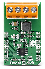
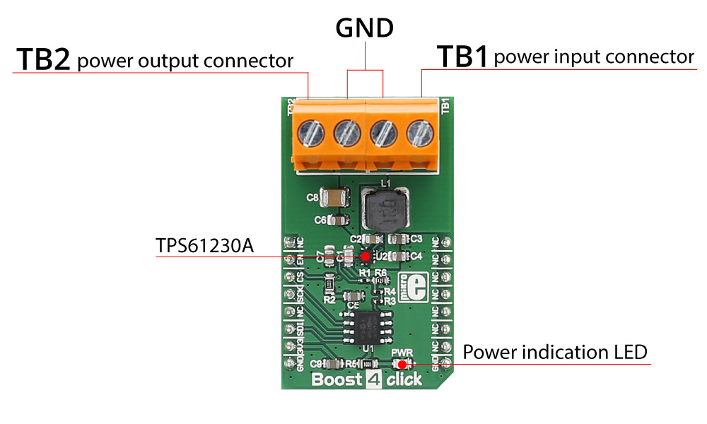
Boost 4 click carries the TPS61230A, a high efficiency fully integrated synchronous boost converter from Texas Instruments. The click is designed to run on a 3.3V power supply. Boost 4 click drives the target chip through the digi pot, which has SPI communication with the microcontroller on the system.
Boost 4 click is the power management solution for your next project.
How the click works
Boost 4 click provides an adjustable output voltage through the SPI DAC, that drives the FB pin to set desired voltage. The click is capable of delivering up to 2.4-A output current at a 5V output with the 2.5-V input supply.
TPS61230A features
The TPS61230A device is a high efficiency fully integrated synchronous boost converter. It integrates 6-A, 21-mO and 18-mO power switches.
During the light load condition, the TPS61230A automatically enters into the PFM operation for maximizing the efficiency with the lowest quiescent current. In the shutdown by pulling EN pin to the logic low, the load is completely disconnected from the input, and the input current consumption is reduced to below 1.0 ??A.
Specifications
| Type |
Boost |
| Applications |
Battery powered products, battery backup units, etc. |
| On-board modules |
TPS61230A, a high efficiency fully
integrated synchronous boost converter from Texas Instruments |
| Key Features |
Input Voltage Range: 2.5 V to 4.5 V, output Voltage Range: 2.5 V to 5.5 V |
| Interface |
SPI |
| Input Voltage |
3.3V |
| Click board size |
M (42.9 x 25.4 mm) |
Pinout diagram
This table shows how the pinout on Boost 4 click corresponds to the pinout on the mikroBUS??? socket (the latter shown in the two middle columns).
| Notes | Pin |  | Pin | Notes |
|---|
|
NC |
1 |
AN |
PWM |
16 |
NC |
|
| Enable pin |
EN |
2 |
RST |
INT |
15 |
NC |
|
| Chip select |
CS |
3 |
CS |
TX |
14 |
NC |
|
| SPI clock |
SCK |
4 |
SCK |
RX |
13 |
NC |
|
|
SDO |
5 |
MISO |
SCL |
12 |
NC |
|
| Slave data in for SPI |
SDI |
6 |
MOSI |
SDA |
11 |
NC |
|
|
NC |
7 |
3.3V |
5V |
10 |
NC |
|
| Ground |
GND |
8 |
GND |
GND |
9 |
GND |
Ground |
Programming
Code examples for Boost 4 click, written for MikroElektronika hardware and compilers are available on Libstock.
Code snippet
The following code snippet shows how to cycle through different output voltages.
01 void main()
02 {
03     systemInit();
04
05    while (1)
06     {
07         delay_ms(3000);
08         //Sets the voltage to VOUTmax, ~5.25 V
09         CS_PIN = 0;       //Sets chip select to active
10         Spi3_Write(0b01110000);
11         Spi3_Write(0b00000000);
12         CS_PIN = 1;       //Sets chip select to inactive
13
14        delay_ms(3000);
15         //Sets the voltage to VOUTmin, which depends on VIN, but cannot
16         //be lower than 2.50 V
17         CS_PIN = 0;       //Sets chip select to active
18         Spi3_Write(0b01111111);
19         Spi3_Write(0b11111111);
20         CS_PIN = 1;       //Sets chip select to inactive
21
22        delay_ms(3000);
23         //Sets the voltage ~4.0 V
24         CS_PIN = 0;       //Sets chip select to active
25         Spi3_Write(0b01110111);
26         Spi3_Write(0b01000000);
27         CS_PIN = 1;       //Sets chip select to inactive
28
29        delay_ms(3000);
30         //Sets the voltage ~4.5 V
31         CS_PIN = 0;       //Sets chip select to active
32         Spi3_Write(0b01110100);
33         Spi3_Write(0b00011111);
34         CS_PIN = 1;       //Sets chip select to inactive
35     }
36 }