The integrated triple buck converter on the Click board™ is labeled as the TPS65263, and it also features overcurrent, overvoltage, thermal, and short circuit protection, as well as other functions that allow safe and reliable operation of the triple buck converter. The TPS65263 uses out-of-phase PWM control, ensuring that no significant input current ripple appears. Two modes of operation (continuous current and pulse-skipping mode) allow optimal efficiency and good performance with any type of load. These features make the 3xBuck click a perfect solution as a power supply for an embedded application, but also as a flexible and reliable power supply for various other types of devices, which require clean and regulated power.
How does it work?
3xBuck click relies on the TPS65263, a triple synchronous step-down converter with programmable dynamic voltage scaling, from Texas Instruments. This IC contains three independent switching sections, which operate at a fixed frequency of 600kHz. One buck section uses the switching clock which is 180° out-of-phase, with respect to other two sections. This ensures low input current ripple, as well as the lowered EMI of the power supply itself.
The TPS65263 IC has the I2C bus logic section, which allows the output voltage of each converter to be programmed. Initially, the output voltage is set with a pair of feedback voltage divider resistors on each section. The output voltages of the sections are set to 5V, 3.3V, and 1.8V because these values are the most commonly used in the embedded applications. As soon as the command is sent via the I2C interface, the logic section of the TPS65263 IC takes over the control, allowing to program the voltage at each of the three outputs between 0.68V to 1.95V, with 10 mV steps. This allows the desired output to be fine-tuned, according to specific needs of the application which is powered by the 3xBuck click. The I2C interface is also used to retrieve the Power Good status, as well as the overcurrent and the die temperature warning for each buck section, independently.
There are three completely independent switching sections in the TPS65263 IC, which means that each has its own dedicated Enable pin, Soft-Start pin, and loop compensation pin. The Enable pins for each section are routed to mikroBUS™. EN1, EN2, and EN3 are routed to AN, PWM and INT pins of the mikroBUS™, respectively. This allows the host MCU to control the operation of the 3xBuck click.
Not all three sections share the same characteristics. The output of the 3xBuck click labeled as 1V8 (VOUT1) can withstand up to 3A of current, while supplied with 12V across the input terminal. Other two outputs can deliver up to 2A, keeping the output well regulated, well within the 1% margin. However, it should be noted that this is the combined current rating, so if multiple outputs are used, the summed current consumption should not exceed these values. The input voltage should range between 4.5V and 18V with a remark that it must be sufficiently higher than the selected output voltage, in order to reach the specified voltage and current ratings.
The soft-start feature is implemented by using a 10nF capacitor at the dedicated SS pin. Each channel has its own dedicated SS pin, so there are three pins in total, used to set the soft-start of each channel. The soft-start function prevents the high inrush current on power up, ramping up the output current during the soft-start period, defined by the capacitor.
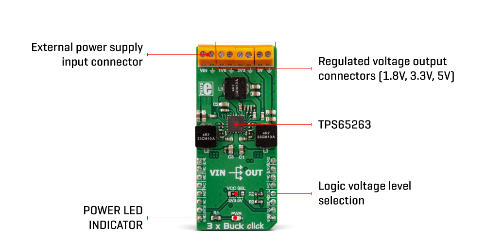
As mentioned before, the device features a set of protecting functions, that allow reliable operation in events such as the short circuit protection, as well as the overcurrent, overvoltage, and thermal protection. If the connected load draws too much current, the cycle-by-cycle current limit will be activated on both the high-side and low-side output MOSFETs. If the high current condition persists after 0.5ms, the device will enter the hiccup mode, shutting down completely, then restarting after 14ms. The whole startup sequence will be repeated and if the fault condition persists on the output, this cycle will be repeated. This prevents damage in a case of significant loads connected at the output. The logic voltage level of the 3xBuck click can be selected by switching the SMD jumper labeled as VCC SEL to an appropriate position. This allows interfacing with both 3.3V and 5V MCUs, expanding the interfacing options of the Click board™.
Specifications
| Type |
Buck |
| Applications |
A regulated power source with three independent outputs, well suited for a wide range of embedded applications, single board systems, general points of load, and similar applications which can benefit from having three most commonly used regulated outputs on a single device |
| On-board modules |
TPS65263, a triple synchronous step-down converter with programmable dynamic voltage scaling, from Texas Instruments |
| Key Features |
Low power dissipation due to high efficiency, three independent converters on a same die, overcurrent, overvoltage and thermal protection, output voltage adjustment over the industry-standard I2C interface, reasonably high current |
| Interface |
I2C |
| Input Voltage |
3.3V,5V |
| Click board size |
M (42.9 x 25.4 mm) |
Pinout diagram
This table shows how the pinout on 3xBuck click corresponds to the pinout on the mikroBUS™ socket (the latter shown in the two middle columns).
| Notes | Pin |  | Pin | Notes |
|---|
| Channel 1 Enable |
EN1 |
1 |
AN |
PWM |
16 |
EN2 |
Channel 2 Enable |
|
NC |
2 |
RST |
INT |
15 |
EN3 |
Channel 3 Enable |
|
NC |
3 |
CS |
RX |
14 |
NC |
|
|
NC |
4 |
SCK |
TX |
13 |
NC |
|
|
NC |
5 |
MISO |
SCL |
12 |
SCL |
I2C Clock |
|
NC |
6 |
MOSI |
SDA |
11 |
SDA |
I2C Data |
| Power supply |
3V3 |
7 |
3.3V |
5V |
10 |
5V |
Power supply |
| Ground |
GND |
8 |
GND |
GND |
9 |
GND |
Ground |
Onboard settings and indicators
| Label | Name | Default | Description |
|---|
| LD1 |
PWR |
- |
Power LED indicator |
| TB1 |
5V |
- |
Regulated 5V voltage output connector |
| TB2 |
3V3 |
- |
Regulated 3.3V voltage output connector |
| TB3 |
1V8 |
- |
Regulated 1.8V voltage output connector |
| TB4 |
VIN |
|
External power supply input connector |
Software support
We provide a library for the 3xBuck Click on our LibStock page, as well as a demo application (example), developed using MikroElektronika compilers. The demo can run on all the main MikroElektronika development boards.
Library Description
The library initializes and defines the I2C bus driver and drivers that offer a choice for writing data in registers and reading data from registers. The library includes functions for set output voltage, enable and disable buck, configuration buck and read buck status.
Key functions:
void c3xbuck_enableBuck(uint8_t buck) - Function for enable Buck
void c3xbuck_setVoltage(uint8_t buck, uint8_t voltage) - Function for set output voltage
void c3xbuck_configurationBuck(uint8_t buck, uint8_t config) - Function for configuration buck
Examples description
The application is composed of the three sections :
- System Initialization - Initializes I2C module and set INT pin, PWM pin and AN pin as OUTPUT
- Application Initialization - Initializes the driver init, enable and configuration Buck 1, Buck 2 and Buck 3c
- Application Task - (code snippet) - Sets variable output voltage and default output voltage
- note: Default output voltage on Buck 1 is 1800mV, Buck 2 is 3300mV and Buck 3 is 5000mV Variable output voltage on all Bucks from 680mV to 1950mV
void applicationTask()
{

    c3xbuck_setVoltage(_C3XBUCK_SELECT_BUCK_1, _C3XBUCK_OUTPUT_VOLTAGE_1000mV);
    c3xbuck_setVoltage(_C3XBUCK_SELECT_BUCK_2, _C3XBUCK_OUTPUT_VOLTAGE_1250mV);
    c3xbuck_setVoltage(_C3XBUCK_SELECT_BUCK_3, _C3XBUCK_OUTPUT_VOLTAGE_1500mV);
    Delay_ms( 5000 );

    c3xbuck_setVoltage(_C3XBUCK_SELECT_BUCK_1, _C3XBUCK_BUCK_DEFAULT_OUTPUT_VOLTAGE);
    c3xbuck_setVoltage(_C3XBUCK_SELECT_BUCK_2, _C3XBUCK_BUCK_DEFAULT_OUTPUT_VOLTAGE);
    c3xbuck_setVoltage(_C3XBUCK_SELECT_BUCK_3, _C3XBUCK_BUCK_DEFAULT_OUTPUT_VOLTAGE);
    Delay_ms( 5000 );

}
The full application code, and ready to use projects can be found on our LibStock page.
Other mikroE Libraries used in the example:
Additional notes and information
Depending on the development board you are using, you may need USB UART click, USB UART 2 click or RS232 click to connect to your PC, for development systems with no UART to USB interface available on the board. The terminal available in all MikroElektronika compilers, or any other terminal application of your choice, can be used to read the message.
mikroSDK
This click board is supported with mikroSDK - MikroElektronika Software Development Kit. To ensure proper operation of mikroSDK compliant click board demo applications, mikroSDK should be downloaded from the LibStock and installed for the compiler you are using.
For more information about mikroSDK, visit the official page.